Every digital transaction, autonomous navigation maneuver, aerospace defense system, and modern telecommunication node relies entirely on integrated circuits measured in nanometers. For decades, the geographical concentration of advanced microelectronics manufacturing left global supply chains vulnerable to physical disruptions and geopolitical volatility.
The construction of massive semiconductor fabrication facilities in the Phoenix metropolitan area, led by Taiwan Semiconductor Manufacturing Company (TSMC), represents one of the largest foreign direct investments in American history. However, building advanced fabrication infrastructure requires more than concrete and cleanroom tools; it requires thousands of highly skilled engineers, material scientists, and equipment technicians.
Arizona State University (ASU) has emerged as the academic engine fueling this industrial revitalization. Through specialized degree tracks, hands-on cleanroom bootcamps, and direct corporate recruitment pipelines, the university provides students with clear pathways into advanced chip manufacturing.
The Global Microelectronics Shift: Why the Phoenix Semiconductor Corridor Matters
Microchips represent the foundational building blocks of the contemporary global economy. From automotive engine management units to cloud data processing arrays, access to cutting-edge silicon determines technological leadership and national economic stability.
Historically, the United States invented the semiconductor industry but gradually offshored the capital-intensive fabrication phase, retaining primarily high-level architectural design and intellectual property development. This created an operational imbalance where domestic manufacturing dropped to approximately ten percent of worldwide chip volume.
The passage of the federal CHIPS and Science Act catalyzed a nationwide reshoring movement. TSMC’s commitment to invest tens of billions of dollars across multiple fabrication plants (commonly called “fabs”) in north Phoenix positioned Arizona as the preeminent microelectronics manufacturing hub in the Western Hemisphere.
Quick Fact: A state-of-the-art semiconductor fabrication plant operates twenty-four hours a day, 365 days a year, requiring an ultra-clean environment up to thousands of times purer than a hospital surgical suite.
Advanced fabrication facilities require a continuous supply of specialized labor across every tier of operation. A single gigafab requires thousands of professionals spanning process development, mechanical integration, high-vacuum maintenance, statistical yield analysis, and supply chain logistics.
ASU sits at the geographical and technical center of this ecosystem, leveraging its research infrastructure to prepare both undergraduate and graduate students for immediate employment in these mission-critical manufacturing facilities.
Understanding Advanced Chip Manufacturing: What Happens Inside a Fab
To grasp the technical competencies required in these careers, one must understand the journey of a silicon wafer through an advanced manufacturing facility. The fabrication process takes raw electronic-grade silicon ingots, slices them into circular discs 300 millimeters in diameter, and constructs billions of interconnected microscopic switches across dozens of patterned layers.
This process takes three to five months from bare substrate to packaged die. It involves hundreds of discrete chemical, physical, and optical steps executed within Class 1 and Class 10 cleanroom environments where airborne particulates are strictly controlled.
The fundamental unit of manufacturing is the cleanroom bay, where automated material handling systems (AMHS) transport front-opening unified pods (FOUPs) filled with wafers along overhead monorail tracks directly into specialized processing tools.
Important: In advanced semiconductor manufacturing, a single dust particle invisible to the human eye can land on a circuit trace, causing an open circuit or electrical short that destroys an entire integrated circuit die.
The primary stages of wafer processing form the core technical domain taught within ASU’s microelectronics curricula:
| Manufacturing Phase | Physical Mechanism | Primary Equipment Involved | Critical Technical Roles |
|---|---|---|---|
| Photolithography | Transfers microscopic circuit geometric patterns onto photoresist using extreme ultraviolet (EUV) or deep ultraviolet (DUV) light. | EUV/DUV Scanners, Track Systems, Reticle Pods | Lithography Process Engineers, Optical Field Engineers |
| Etch (Dry and Wet) | Removes unprotected layers of silicon dioxide, polysilicon, or metal using reactive gas plasmas or chemical solvents. | Plasma Reactive Ion Etchers (RIE), Wet Chemical Benches | Etch Yield Specialists, Plasma Physics Technicians |
| Thin Film Deposition | Grows or deposits atomic-scale insulating and conducting films via chemical vapor deposition (CVD) or atomic layer deposition (ALD). | Atomic Layer Deposition Chambers, Sputtering Systems | Thin Films Process Engineers, Vacuum Technicians |
| Chemical Mechanical Planarization (CMP) | Polishes the wafer surface flat at the angstrom level using chemical slurries and mechanical abrasive pads between metal layers. | Rotary Polishing Platens, Slurry Dispense Loops | CMP Yield Engineers, Slurry Chemistry Technicians |
| Ion Implantation & Diffusion | Bombards selected silicon regions with dopant atoms (boron, phosphorus, arsenic) to alter local electrical conductivity. | High-Current Ion Implanters, Thermal Annealing Furnaces | Doping Process Engineers, High-Voltage Equipment Techs |
| Metrology & Inspection | Measures critical dimensions, thin-film thicknesses, and detects sub-nanometer physical defects on active production wafers. | Scanning Electron Microscopes (SEM), Ellipsometers | Defect Metrology Engineers, Quality Control Analysts |
Mastering these interconnected physical processes requires foundational knowledge in thermodynamics, fluid dynamics, plasma physics, and materials science. ASU’s programs are built specifically around this operational matrix.
The ASU Academic Framework: Fulton Schools of Engineering and Beyond
Arizona State University’s microelectronics education is anchored by the Ira A. Fulton Schools of Engineering, the largest engineering enterprise in the United States. Rather than treating chip manufacturing as an isolated subfield of electrical engineering, ASU distributes microelectronics training across multiple interdisciplinary schools.
This distributed model reflects modern industry realities. An operational semiconductor plant does not hire only electrical circuit designers; it recruits chemical engineers to manage toxic gases and slurries, mechanical engineers to maintain complex robotic vacuum mechanisms, and industrial engineers to optimize wafer transit flow.
The primary academic units driving semiconductor workforce development include:
- School of Electrical, Computer and Energy Engineering (ECEE): Focuses on device physics, integrated circuit layout design, solid-state electronics, and advanced signal processing.
- School for Engineering of Matter, Transport and Energy (SEMTE): Delivers instruction in chemical engineering, materials science, and mechanical systems essential for thin-film deposition, chemical slurries, and thermal dynamics.
- School of Computing and Augmented Intelligence (SCAI): Prepares students to build automated manufacturing software, yield-optimization analytics, and digital twin models for fab operations.
- The Polytechnic School: Delivers hands-on manufacturing engineering, robotics, automation control, and applied equipment maintenance degrees focused on field readiness.
Expert Tip: When choosing an undergraduate degree path for semiconductor manufacturing, remember that mechanical, chemical, and materials science degrees are just as actively recruited by chip fabs as electrical engineering degrees.
In addition to traditional four-year degrees, ASU offers specialized certificates in semiconductor processing. These credentials enable students in related STEM disciplines—such as physics, chemistry, or industrial mathematics—to demonstrate targeted cleanroom and fabrication literacy to corporate recruiters.
World-Class Cleanroom Facilities: ASU NanoFab and MacroTechnology Works
One of the greatest barriers in microelectronics education is the astronomical cost of physical cleanroom infrastructure. Most universities teach semiconductor theory exclusively on blackboards or computer simulations because operating a live fabrication environment costs millions of dollars annually.
ASU overcomes this limitation through two world-class research and training complexes: the ASU NanoFab on the Tempe campus and the MacroTechnology Works (MTW) facility at the ASU Research Park.
The ASU NanoFab is a premier open-access facility housing Class 100 and Class 1,000 cleanroom bays. Equipped with tools for optical lithography, reactive ion etching, physical vapor deposition, and electron-beam metrology, the facility allows undergraduate students to fabricate working devices with their own hands.
Pro Tip: Completing the safety training and equipment qualification modules at the ASU NanoFab during your sophomore or junior year instantly elevates your resume above thousands of applicants who have only textbook knowledge.
MacroTechnology Works represents an even larger industrial-scale resource. Originally constructed as an advanced research and development fabrication plant by Motorola, MTW houses high-bay cleanroom infrastructure capable of processing 200mm and 300mm silicon wafers.
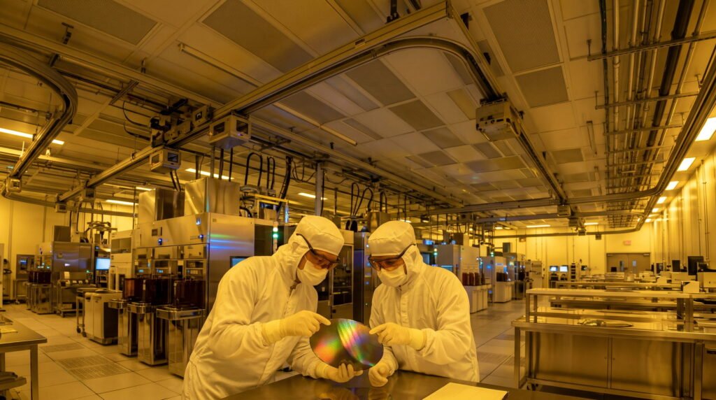
This enterprise-grade footprint allows the university to replicate the exact physical operational conditions students will encounter in commercial high-volume manufacturing facilities. Students learn how to navigate air showers, gown up in full cleanroom suits, handle toxic gas protocols, and operate heavy industrial process tools.
| Facility Feature | ASU NanoFab (Tempe Campus) | MacroTechnology Works (ASU Research Park) |
|---|---|---|
| Primary Focus | Academic research, device prototyping, undergraduate lab training | Industrial-scale pilot manufacturing, workforce bootcamps, joint R&D |
| Cleanroom Classification | Class 100, Class 1,000, and Class 10,000 bays | High-bay Class 10, Class 100, and Class 1,000 clean spaces |
| Wafer Handling Capabilities | Individual piece parts up to 150mm/200mm wafers | Industrial-standard 200mm and 300mm wafer processing lines |
| Core Equipment Sets | Optical aligners, metal evaporators, thermal oxidizers, profilometers | Advanced photolithography tracks, industrial plasma etchers, CMP tools |
| Primary Student Access | Enrolled lab coursework, independent study, FURI projects | Specialized workforce training, corporate co-ops, graduate research |
The Technician and Engineering Pathways: Two Distinct Career Routes
Employment within advanced semiconductor manufacturing splits into two primary, interconnected career tracks: the Engineering Pathway and the Manufacturing Equipment Technician Pathway. Both tracks are vital, offer lucrative compensation, and experience severe talent shortages.
Understanding the differences in educational requirements, daily tasks, and career trajectories helps students choose the path that best matches their aptitudes and professional goals.
The Engineering Pathway
The engineering pathway typically requires a minimum of a Bachelor of Science (B.S.), Master of Science (M.S.), or Ph.D. in an engineering or physical science discipline. Engineers are responsible for process optimization, defect reduction, recipe development, and technological integration.
A Process Engineer, for example, monitors statistical process control (SPC) charts for a specific fab module like photolithography or chemical mechanical planarization. When wafer yield dips or critical dimensions drift beyond allowable nanometer tolerances, the engineer conducts root-cause investigations and adjusts chemical or optical parameters.
The Equipment Technician Pathway
The technician pathway focuses on the physical maintenance, mechanical assembly, calibration, and troubleshooting of multimillion-dollar cleanroom machinery. Technicians often enter the field through specialized Associate degrees, military technical service, or accelerated university certification bootcamps.
An Equipment Maintenance Technician works inside the cleanroom, donning protective suits to service robotic arms, replace radio-frequency plasma generators, rebuild cryogenic vacuum pumps, and execute preventive maintenance schedules to maximize tool uptime.
| Career Parameter | Manufacturing Equipment Technician | Semiconductor Process Engineer |
|---|---|---|
| Entry-Level Education | Associate of Applied Science (AAS) or Specialized Certificate | Bachelor of Science (B.S.) or Master of Science (M.S.) |
| Daily Operational Focus | Mechanical troubleshooting, preventive tool maintenance, parts replacement | Statistical process control, recipe adjustment, defect analysis, yield modeling |
| Primary Work Environment | 100% inside cleanroom, hands-on mechanical interaction with tools | Balanced between cleanroom investigation, office analysis, and cross-team meetings |
| Key Skillset | Electro-mechanical diagnostics, vacuum systems, pneumatics, schematics | Advanced mathematics, materials chemistry, Python/R, experimental design |
| Typical Work Schedule | Compressed workweek shifts (e.g., alternating 3-day/4-day 12-hour shifts) | Standard business hours with rotating on-call support for fab line emergencies |
| Average Starting Salary Range | $60,000 – $85,000 (plus overtime and shift differentials) | $85,000 – $115,000 (plus annual bonuses and equity) |
Collaborative Training Programs and Fast-Track Industry Bootcamps
Addressing the massive workforce deficit requires rapid-skilling programs in addition to traditional multi-year degree pathways. ASU, often working alongside the Maricopa County Community College District (MCCCD), has developed accelerated training programs designed to quickly prepare candidates for cleanroom entry.
The Quick Start program represents a prime example of this agile educational philosophy. Designed as an intensive, hands-on bootcamp, this program teaches adult learners, career changers, and university underclassmen the foundational competencies needed to become semiconductor manufacturing technicians in just two weeks.
Quick Fact: The Semiconductor Quick Start program covers cleanroom protocol, electrostatic discharge (ESD) safety, pneumatic systems, vacuum theory, and mechanical lock-out/tag-out procedures through intensive laboratory practice.
Participants learn the physical mechanics of semiconductor maintenance by dismantling and rebuilding real vacuum valves, wiring industrial sensors, and practicing gowning procedures in simulated clean environments.
Upon successful completion of the bootcamp, participants earn an industry-recognized credential and are guaranteed an interview with participating semiconductor employers in the Phoenix valley. This program serves as an accessible on-ramp into high-tech manufacturing without requiring years of prior academic debt.
Advanced Degree Specializations and Applied Research Opportunities
For students pursuing graduate studies, Arizona State University offers research environments that work directly on the operational frontiers of the semiconductor industry. These advanced programs focus on overcoming the physical limitations of classical transistor scaling.
Through master’s applied projects and doctoral dissertations, graduate researchers collaborate with faculty on active grants funded by the National Science Foundation, the Department of Defense, and private microelectronics consortia.
Major areas of graduate specialization include:
- Extreme Ultraviolet (EUV) and Next-Generation Lithography: Investigating photoresist chemical dynamics, pellicle durability, and optical aberration correction at sub-two-nanometer dimensions.
- Advanced Packaging and Heterogeneous Integration: Developing 2.5D and 3D chiplet stacking techniques that combine memory and processing dies within a single package to bypass interconnect bottlenecks.
- Wide-Bandgap Semiconductors: Synthesizing and etching gallium nitride (GaN) and silicon carbide (SiC) devices for high-voltage power electronics and electric vehicle power trains.
- Cryogenic and Quantum Electronics: Designing specialized silicon structures capable of operating at near absolute zero to interface with quantum computing processors.
Pro Tip: Graduate students supported through corporate-sponsored research fellowships often have their tuition fully covered and receive a living stipend while gaining direct access to proprietary industrial datasets.
These advanced degrees prepare graduates for elite career tracks, such as Senior Yield Integration Manager, Device Physics Architect, and Advanced Technology Director, commanding significant influence over future product roadmaps.
The Southwest Advanced Prototyping (SWAP) Hub
Workforce readiness and manufacturing capability are directly tied to national security. In response to federal initiatives establishing microelectronics commons hubs across the country, Arizona State University was selected to lead the Southwest Advanced Prototyping (SWAP) Hub.
The SWAP Hub operates as a rapid prototyping center connecting university laboratories directly to defense agencies and commercial fabrication foundries. Its core mission is to bridge the “lab-to-fab” valley of death—the notorious stage where promising laboratory discoveries fail to transition into commercial-scale manufacturing lines.
For students, the existence of the SWAP Hub provides unprecedented educational benefits:
- Direct Defense and Commercial Prototyping: Students work on real hardware prototypes addressing secure microelectronics, electromagnetic sensors, and edge-computing microchips.
- Paid Research Apprenticeships: Undergraduate and graduate researchers receive institutional funding to maintain cleanroom tools, develop fabrication recipes, and test device packaging.
- Inter-Institutional Networking: The hub connects ASU students with researchers at partner universities, such as the University of Arizona and Northern Arizona University, and scientists at national laboratories.
- Commercial Translation Exposure: Students see firsthand how microelectronic intellectual property is evaluated, patented, and packaged for commercial licensing.
This massive federal footprint ensures that students graduating from ASU understand not just theoretical physics, but the rigid regulatory, quality, and security frameworks governing defense-grade semiconductor manufacturing.
Step-by-Step Guide: How an ASU Student Transitions into a Chip Manufacturing Career
Securing a position at a tier-one manufacturing foundry requires disciplined planning from the beginning of your academic career. With thousands of students enrolled in engineering programs, intentional milestones are essential to stand out to corporate recruiters.
Follow this proven four-year roadmap to navigate from enrollment to an engineering or technician role:
- Year One: Establish Foundational CompetenceFocus intensively on mastering core calculus, differential equations, physics, and introductory programming in Python or C++. Attend engineering student organizations such as IEEE (Institute of Electrical and Electronics Engineers) or MRS (Materials Research Society) to learn about industry trends and connect with upperclassmen.
- Year Two: Secure Cleanroom and Safety CredentialsComplete safety onboarding for the ASU NanoFab. Take elective courses that introduce semiconductor properties and vacuum technology. Apply for the Fulton Undergraduate Research Initiative (FURI) to secure faculty mentorship and hands-on laboratory experience early in your undergraduate studies.
- Year Three: Pursue Specialized Coursework and InternshipsEnroll in upper-division courses covering photolithography, solid-state devices, and statistical quality control. Attend the university’s specialized microelectronics career fairs held every fall and spring. Secure an engineering internship or co-op with local fab operators or equipment suppliers.
- Year Four: Complete Capstone Projects and Final RecruitmentSelect an industry-sponsored capstone design project that directly tackles an active manufacturing problem, such as wafer defect classification or thermal dissipation. Complete formal job interviews with semiconductor recruiters during the early fall semester, securing full-time job offers well before spring graduation.
Common Mistake: Waiting until your final semester to apply for semiconductor jobs without prior cleanroom or laboratory exposure puts you at a severe disadvantage. Companies prioritize candidates with verified hands-on experience in sterile environments.
Overcoming Challenges: What to Expect in the Fab Environment
While careers in advanced semiconductor manufacturing offer stability, competitive pay, and cutting-edge technical challenges, students must understand the realities of the working environment before committing to this industry.
A manufacturing fab is an intense, fast-paced industrial environment governed by strict discipline. Equipment downtime can cost hundreds of thousands of dollars per hour, creating high-pressure conditions when unexpected yield drops or tool failures occur.
Key operational challenges in advanced chip manufacturing include:
- Strict Cleanroom Protocols: Personnel must spend extended hours inside full protective cleanroom garments (“bunny suits”), including gloves, hoods, boots, and face masks. Cosmetics, perfumes, and unapproved writing materials are strictly forbidden inside the facility.
- Compressed Work Schedules: Many fab roles, particularly for technicians and module shift engineers, follow alternating compressed work schedules (such as three 12-hour shifts one week, followed by four 12-hour shifts the next, including night shifts and weekends).
- Rigorous Safety Mandates: Processing microchips requires hazardous gases (such as silane, arsine, and phosphine), corrosive acids, and high-voltage power supplies. Adherence to safety protocols must be flawless at all times.
- Cross-Cultural Communication: Global foundries operate with multinational teams, requiring strong cultural awareness, patience, and clear technical communication across different languages and working styles.
Warning: Working in cleanrooms requires standing, walking, and bending for long periods while wearing multi-layered protective gear under yellow-tinted cleanroom lighting. Candidates should ensure they are comfortable in enclosed, highly structured environments.
For individuals who thrive on systematic problem-solving, real-time troubleshooting, and tangible physical outcomes, these operational realities provide a deeply rewarding, highly collaborative professional life.
Long-Term Career Trajectories and Industry Compensation
The global demand for microchips ensures that expertise in advanced semiconductor manufacturing remains one of the most recession-resilient career fields in engineering. As chip fabrication scales across Arizona, career progression pathways continue to expand.
Professionals entering the field often move between operational, design, and strategic corporate leadership roles over the course of their careers:
| Career Milestone | Typical Job Titles | Key Responsibilities | Average Annual Base Compensation |
|---|---|---|---|
| Entry-Level (0–3 Years) | Associate Process Engineer, Equipment Technician II, Yield Analyst | Tool calibration, baseline recipe execution, routine defect inspection, preventative maintenance | $70,000 – $95,000 |
| Mid-Career (4–8 Years) | Senior Module Engineer, Cleanroom Shift Supervisor, Metrology Lead | New tool installation, process parameter optimization, managing technician crews, vendor management | $100,000 – $135,000 |
| Senior / Staff (8–15 Years) | Principal Integration Engineer, Fab Operations Manager, Director of Yield | Cross-module integration, next-node technology transfer, capital expenditure planning, site safety oversight | $140,000 – $190,000 |
| Executive Leadership (15+ Years) | Vice President of Manufacturing, Site General Manager, Chief Technology Officer | Multi-fab site governance, corporate capacity expansion, executive client relations, strategic supply chain alignment | $200,000 – $350,000+ (plus executive stock packages) |
Beyond working directly for chip manufacturers, graduates can leverage their cleanroom and processing skills across a vast supporting ecosystem. Major equipment vendors (such as ASML, Applied Materials, Lam Research, and KLA) actively recruit ASU graduates to commission, service, and optimize their multi-million-dollar toolsets inside the fabs.
Frequently Asked Questions
Do I need to be an Electrical Engineering major to work at a semiconductor fabrication facility?
No. Semiconductor manufacturing requires diverse engineering disciplines. Mechanical engineers are needed to manage complex robotics and vacuum chambers; chemical engineers manage thin-film deposition and toxic gas distribution; materials scientists optimize wafer substrates; and industrial engineers design efficient wafer routing flows across the fab floor.
What is the minimum degree required to get a job at a semiconductor manufacturing plant?
Technician roles require a high school diploma or GED combined with a specialized certificate (like the Semiconductor Quick Start bootcamp) or an Associate of Applied Science (AAS) degree. Process engineering, integration, and research roles typically require a Bachelor of Science (B.S.), Master of Science (M.S.), or Ph.D. in an engineering or physical science discipline.
How does the ASU NanoFab prepare students for commercial fabs?
The ASU NanoFab teaches students real-world cleanroom discipline, gowning protocols, chemical safety, and tool operation. Handling physical silicon wafers, running photolithography aligners, and operating plasma etchers inside a live research cleanroom eliminates the initial learning curve when entering commercial manufacturing facilities.
Can international students enrolled at ASU work in the Arizona semiconductor industry?
Yes. International students in STEM degree programs can utilize Curricular Practical Training (CPT) for internships and Optional Practical Training (OPT) for up to three years of post-graduation employment in the United States. However, certain specialized research projects connected to national defense or ITAR regulations may be restricted to United States citizens.
What is the difference between semiconductor design and semiconductor manufacturing?
Semiconductor design (fabless) focuses on conceptualizing and simulating electronic circuits using computer-aided design software to create the logical blueprint for a chip. Semiconductor manufacturing (foundry) takes those digital blueprints and physically constructs the physical devices on silicon wafers through chemical, optical, and physical cleanroom processes.
What is the Quick Start program and how do I enroll?
The Quick Start program is an accelerated two-week training bootcamp delivered in partnership with local community colleges and university partners. It teaches foundational cleanroom safety, vacuum mechanics, hand-tool usage, and manufacturing literacy, culminating in direct job interviews with local chip manufacturing employers.
Is working inside a cleanroom safe given the chemicals and gases involved?
Modern semiconductor fabrication plants are among the most strictly regulated and monitored industrial workplaces in the world. Extensive air scrubbers, automated toxic gas sniffers, continuous laminar airflow, chemical personal protective equipment, and rigid interlocks ensure that working inside a cleanroom is exceptionally safe.
How does the CHIPS Act directly help ASU students?
The CHIPS Act provides billions of dollars in federal funding to expand domestic microelectronics research facilities, fund student engineering scholarships, support faculty research grants, and build regional prototyping hubs like the Southwest Advanced Prototyping (SWAP) Hub led by ASU.
What is a compressed work schedule in a manufacturing fab?
Because fabs operate continuously, technicians and shift engineers often work compressed 12-hour shifts. A common format is working three days on, followed by four days off one week, and then four days on, followed by three days off the next week, allowing employees to enjoy extended blocks of personal time off.
Can I tour the cleanroom facilities at ASU before enrolling?
Yes. The Ira A. Fulton Schools of Engineering regularly hosts prospective student tours, engineering open houses, and laboratory showcases. Visitors can view the cleanroom bays through protective exterior observation windows and meet faculty and students working inside the facility.
What are the primary programming languages used in chip manufacturing?
Python is the industry standard for statistical process control, yield optimization scripts, and automated data analysis. C and C++ are widely used for low-level equipment control, tool driver integration, and real-time sensor processing across cleanroom machinery.
How do advanced packaging careers differ from front-end wafer fabrication?
Front-end wafer fabrication constructs the microscopic transistors and metal interconnects directly on raw silicon wafers inside ultra-clean environments. Advanced packaging (back-end) cuts those completed wafers into individual dies, stacks multiple dies together in complex three-dimensional arrangements, and encapsulates them into rugged, finished microchips ready for circuit board assembly.
Conclusion: Building the Post-Silicon Workforce
The re-emergence of advanced semiconductor manufacturing in the United States represents an industrial and educational transformation. The multi-billion-dollar investments anchoring the Phoenix technology corridor have permanently changed the economic landscape of Arizona, positioning it as a cornerstone of the global electronics supply chain.
Arizona State University serves as the critical bridge connecting aspiring professionals to this expanding industry. By providing access to world-class cleanrooms at the NanoFab and MacroTechnology Works, offering interdisciplinary engineering degrees, and leading regional initiatives like the SWAP Hub, ASU provides students with the practical and theoretical foundation necessary to lead in microelectronics.
Whether your goal is to master physical equipment troubleshooting as a cleanroom technician, optimize atomic-layer deposition as a process engineer, or develop revolutionary chiplet architectures in a graduate laboratory, the pathway is established. The global future of technology is being manufactured atom by atom on the silicon wafers of Arizona—and the opportunity to help build that future begins today.